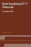
Semi-Insulating III–V Materials: Nottingham 1980
The study of deep levels in semiconductors has seen considerable growth in recent years. Many new techniques have become available for investigating both the electronic properties of deep levels and the chemical nature of the defects from which they arise. This increasing interest has been stimulated by the importance of the subject to device technology, in particular those microwave and opto-electronic devices made from GaAs, InP and their alloys. While previous conferences have covered specialist areas of deep level technology, the meeting described here was arranged to draw together workers from these separate fields of study. The following papers reflect the breadth of interests represented at the conference. For the sake of uniformity we have chosen the English alternative where an American expression has been used. We have also sought to improve grammar, sometimes without the approval of the author in the interests of rapid publication. The Editor wishes to thank the referees for their ready advice at all stages, Paul Jay who helped with many of the editorial duties and Muriel Howes and Lorraine Jones for rapid and accurate typing.
-
Autore:
-
Editore:
-
Anno:2012
-
Rilegatura:Paperback / softback
-
Pagine:361 p.
Le schede prodotto sono aggiornate in conformità al Regolamento UE 988/2023. Laddove ci fossero taluni dati non disponibili per ragioni indipendenti da Feltrinelli, vi informiamo che stiamo compiendo ogni ragionevole sforzo per inserirli. Vi invitiamo a controllare periodicamente il sito www.lafeltrinelli.it per eventuali novità e aggiornamenti.
Per le vendite di prodotti da terze parti, ciascun venditore si assume la piena e diretta responsabilità per la commercializzazione del prodotto e per la sua conformità al Regolamento UE 988/2023, nonché alle normative nazionali ed europee vigenti.
Per informazioni sulla sicurezza dei prodotti, contattare productsafety@feltrinelli.it


